<Back to Index>
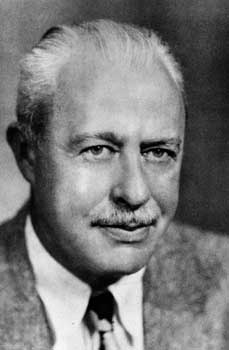
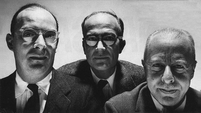
- Physicist Walter Houser Brattain, 1902
- Author Boris Leonidovich Pasternak, 1890
- Prime Minister of the United Kingdom Maurice Harold Macmillan, 1894
PAGE SPONSOR


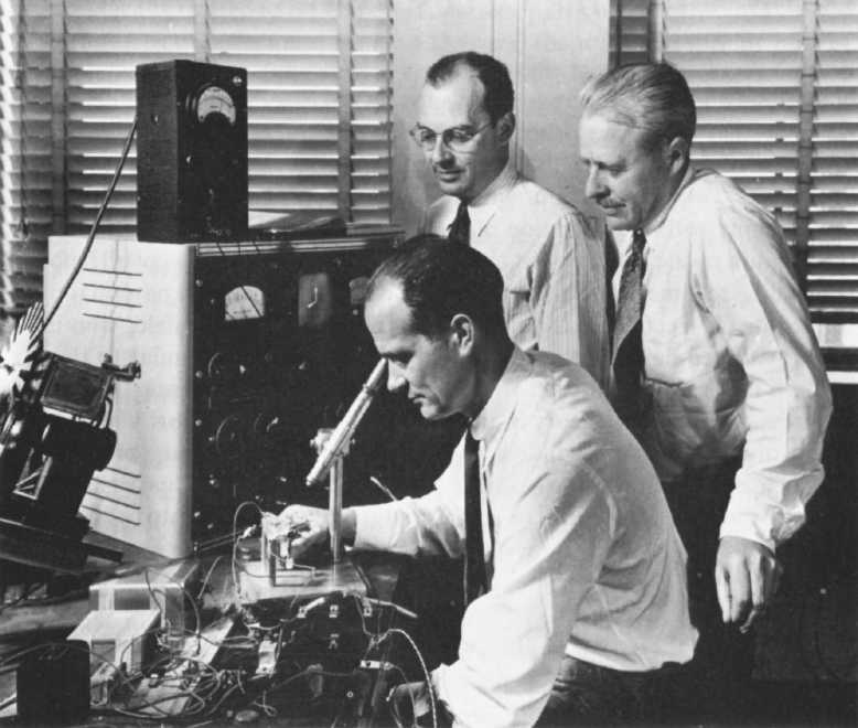
Walter Houser Brattain (February 10, 1902 – October 13, 1987) was an American physicist at Bell Labs who, along with John Bardeen and William Shockley, invented the transistor. They shared the 1956 Nobel Prize in Physics for their invention. He devoted much of his life to research on surface states.
He was born to Ross R. Brattain and Ottilie Houser in Amoy, China, on February 10, 1902 and spent the early part of his life in Springfield, Oregon, and Tonasket, Washington, in the United States. He was raised in Tonasket, Washington, on a cattle ranch owned by his parents, and earned his B.S. degree in physics and mathematics at Whitman College in Walla Walla, Washington. Brattain earned that degree in 1924 and an M.A. degree from the University of Oregon in 1926. He then moved eastward, taking his Ph.D. degree in physics at the University of Minnesota in 1929. Brattain's advisor was John T. Tate, and his thesis was on electron impact in mercury vapor. In 1928 and 1929 he worked at the National Bureau of Standards in Washington, D.C., and in 1929 was hired by Bell Telephone Laboratories.
Brattain's concerns at Bell Laboratories in the years before World War II were first in the surface physics of tungsten and
later in the surfaces of the semiconductors cuprous oxide and silicon.
During World War II Brattain devoted his time to developing methods of
submarine detection under a contract with the National Defense Research
Council at Columbia University. Following the war, Brattain returned to Bell Laboratories and soon joined the semiconductor division of the newly-organized Solid State Department of the laboratories. William Shockley was
the director of the semiconductor division, and early in 1946 he
initiated a general investigation of semiconductors that was intended
to produce a practical solid state amplifier. Crystals of pure semiconductors (such as silicon or germanium)
are very poor conductors at ambient temperatures because the energy
that an electron must have in order to occupy a conduction energy level
is considerably greater than the thermal energy available to an
electron in such a crystal. Heating a semiconductor can excite
electrons into conduction states, but it is more practical to increase
conductivity by adding impurities to the crystal. A crystal may be
doped with a small amount of an element having more electrons than the
semiconductor, and those excess electrons will be free to move through
the crystal; such a crystal is an n-type semiconductor. One may also
add to the crystal a small amount of an element having fewer electrons
than the semiconductor, and the electron vacancies, or holes, so
introduced will be free to move through the crystal like
positively-charged electrons; such a doped crystal is a p-type
semiconductor. At
the surface of a semiconductor the level of the conduction band can be
altered, which will increase or decrease the conductivity of the
crystal. Junctions between metals and n-type or p-type semiconductors,
or between the two types of semiconductors, have asymmetric conduction
properties, and semiconductor junctions can therefore be used to
rectify electrical currents. In a rectifier, a voltage bias that
produces a current flow in the low-resistance direction is a forward
bias, while a bias in the opposite direction is a reverse bias. Semiconductor
rectifiers were familiar devices by the end of World War II, and
Shockley hoped to produce a new device that would have a variable
resistance and hence could be used as an amplifier. He proposed a
design in which an electric field was applied across the thickness of a
thin slab of a semiconductor. The conductivity of the semiconductor
changed only by a small fraction of the expected amount when the field
was applied, which John Bardeen (another
member of Shockley's division) suggested was due to the existence of
energy states for electrons on the surface of the semiconductor.
